
Analysis of dislocation structure in SiC crystal by ray tracing simulation assisted by X-ray topological imaging
Research background
Application importance of silicon carbide (SiC): As a wide bandgap semiconductor material, silicon carbide has attracted much attention due to its excellent electrical properties (such as larger bandgap, higher electron saturation velocity and thermal conductivity). These properties make it widely used in high-frequency, high-temperature and high-power device manufacturing, especially in the field of power electronics.
Influence of crystal defects: Despite these advantages of SiC, defects in crystals remain a major problem hindering the development of high-performance devices. These defects may cause device performance degradation and affect device reliability.X-ray topological imaging technology: In order to optimize crystal growth and understand the impact of defects on device performance, it is necessary to characterize and analyze the defect configuration in SiC crystals. X-ray topological imaging (especially using synchrotron radiation beams) has become an important characterization technique that can produce high-resolution images of the internal structure of the crystal.
Research ideas
Based on ray tracing simulation technology: The article proposes the use of ray tracing simulation technology based on the orientation contrast mechanism to simulate the defect contrast observed in actual X-ray topological images. This method has been proven to be an effective way to study the properties of crystal defects in various semiconductors.Improvement of simulation technology: In order to better simulate the different dislocations observed in 4H-SiC and 6H-SiC crystals, the researchers improved the ray tracing simulation technology and incorporated the effects of surface relaxation and photoelectric absorption.
Research content
Dislocation type analysis: The article systematically reviews the characterization of different types of dislocations (such as screw dislocations, edge dislocations, mixed dislocations, basal plane dislocations and Frank-type dislocations) in different polytypes of SiC (including 4H and 6H) using ray tracing simulation technology.Application of simulation technology: The application of ray tracing simulation technology under different beam conditions such as weak beam topology and plane wave topology, as well as how to determine the effective penetration depth of dislocations through simulation technology are studied.Combination of experiments and simulations: By comparing the experimentally obtained X-ray topological images with the simulated images, the accuracy of the simulation technology in determining the dislocation type, Burgers vector and the spatial distribution of dislocations in the crystal is verified.
Research conclusions
Effectiveness of simulation technology: The study shows that ray tracing simulation technology is a simple, non-destructive and unambiguous method to reveal the properties of different types of dislocations in SiC and can effectively estimate the effective penetration depth of dislocations.3D dislocation configuration analysis: Through simulation technology, 3D dislocation configuration analysis and density measurement can be performed, which is crucial for understanding the behavior and evolution of dislocations during crystal growth.Future applications: Ray tracing simulation technology is expected to be further applied to high-energy topology as well as laboratory-based X-ray topology. In addition, this technology can also be extended to the simulation of defect characteristics of other polytypes (such as 15R-SiC) or other semiconductor materials.
Figure Overview
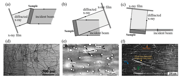
Fig. 1: Schematic diagram of synchrotron radiation X-ray topological imaging setup, including transmission (Laue) geometry, reverse reflection (Bragg) geometry, and grazing incidence geometry. These geometries are mainly used to record X-ray topological images.
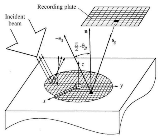
Fig. 2: Schematic diagram of X-ray diffraction of the distorted area around the screw dislocation. This figure explains the relationship between the incident beam (s0) and the diffracted beam (sg) with the local diffraction plane normal (n) and the local Bragg angle (θB).
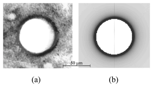
Fig. 3: Back-reflection X-ray topography images of micropipes (MPs) on a 6H–SiC wafer and the contrast of a simulated screw dislocation (b = 6c) under the same diffraction conditions.
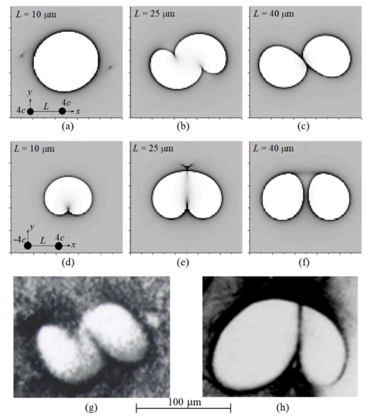
Fig. 4: Micropipe pairs in a back-reflection topography image of a 6H–SiC wafer. Images of the same MPs with different spacings and MPs in opposite directions are shown by ray tracing simulations.
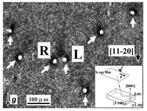
Fig. 5: Grazing incidence X-ray topography images of closed-core screw dislocations (TSDs) on a 4H–SiC wafer are shown. The images show enhanced edge contrast.
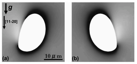
Fig. 6: Ray tracing simulations of grazing incidence X-ray topography images of left-handed and right-handed 1c TSDs on a 4H–SiC wafer are shown.
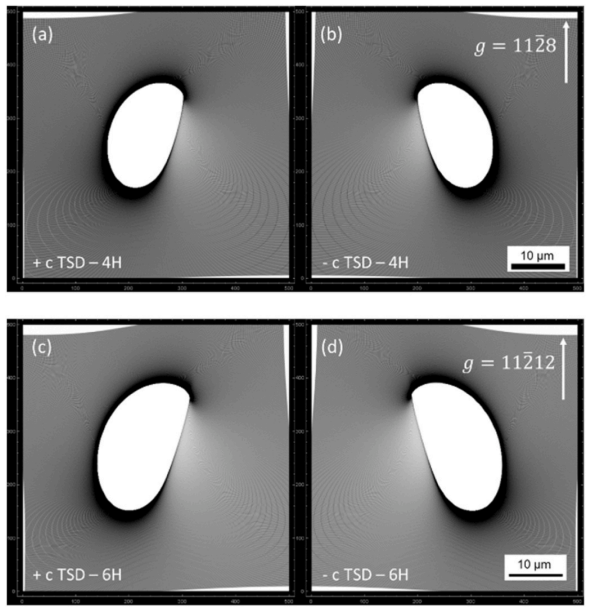
Fig. 7: Ray tracing simulations of TSDs in 4H–SiC and 6H–SiC are shown, showing dislocations with different Burgers vectors and polytypes.
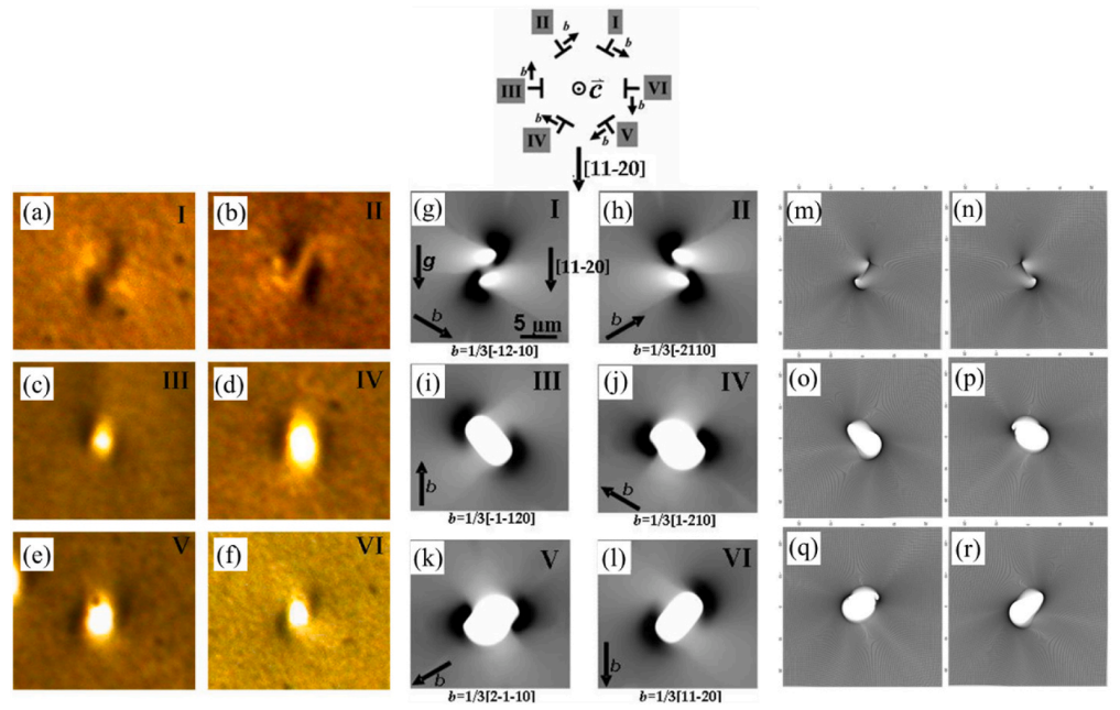
Fig. 8: Shows the grazing incidence X-ray topological images of different types of threading edge dislocations (TEDs) on 4H-SiC wafers, and the TED topological images simulated using the ray tracing method.
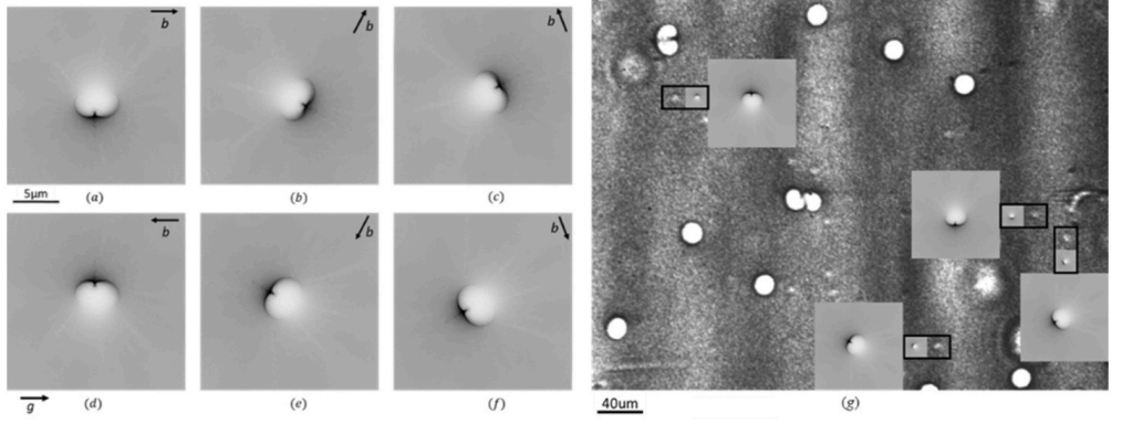
Fig. 9: Shows the X-ray back-reflection topological images of various TED types on 4H-SiC wafers, and the simulated TED contrast.
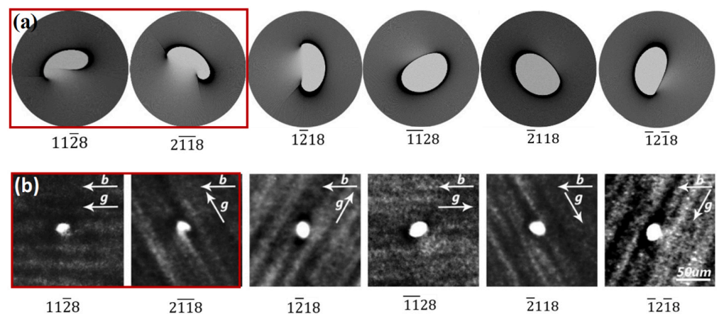
Fig. 10: Shows the ray tracing simulation images of mixed threading dislocations (TMDs) with specific Burgers vectors, and the experimental topological images.
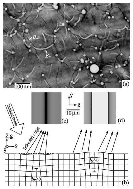
Fig. 11: Shows the back-reflection topological images of basal plane dislocations (BPDs) on 4H-SiC wafers, and the schematic diagram of the simulated edge dislocation contrast formation.
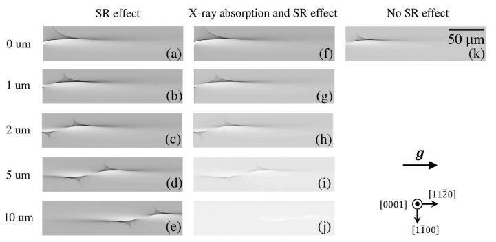
Fig. 12: Shows the ray tracing simulation images of right-handed helical BPDs at different depths considering surface relaxation and photoelectric absorption effects.
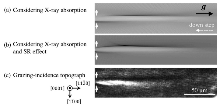
Fig. 13: Shows the ray tracing simulation images of right-handed helical BPDs at different depths, and the grazing incidence X-ray topological images.
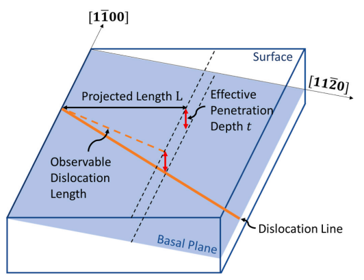
Fig. 14: Shows the schematic diagram of basal plane dislocations in any direction on 4H-SiC wafers, and how to determine the penetration depth by measuring the projection length.
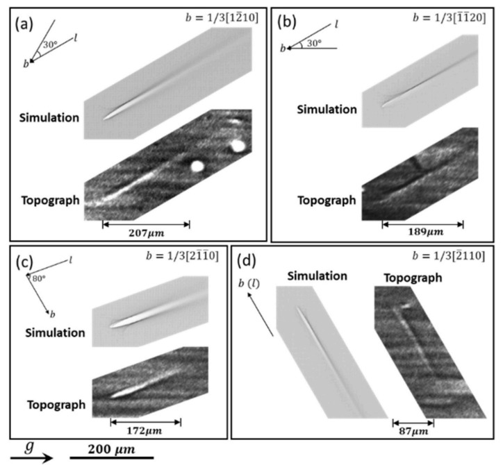
Fig. 15: The contrast of BPDs with different Burgers vectors and line directions in the grazing incidence X-ray topological images, and the corresponding ray tracing simulation results.
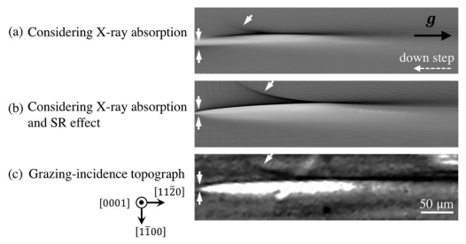
Fig. 16: The ray tracing simulation image of the right-handed deflected TSD on the 4H-SiC wafer, and the grazing incidence X-ray topological image are shown.
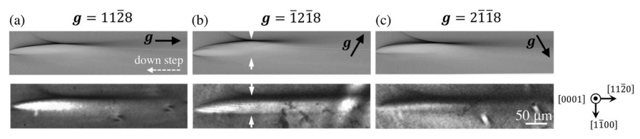
Fig. 17: The ray tracing simulation and experimental image of the deflected TSD on the 8° offset 4H-SiC wafer are shown.
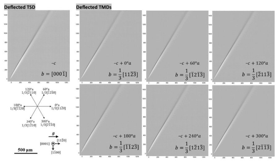
Fig. 18: The ray tracing simulation images of the deflected TSD and TMDs with different Burgers vectors but the same line direction are shown.
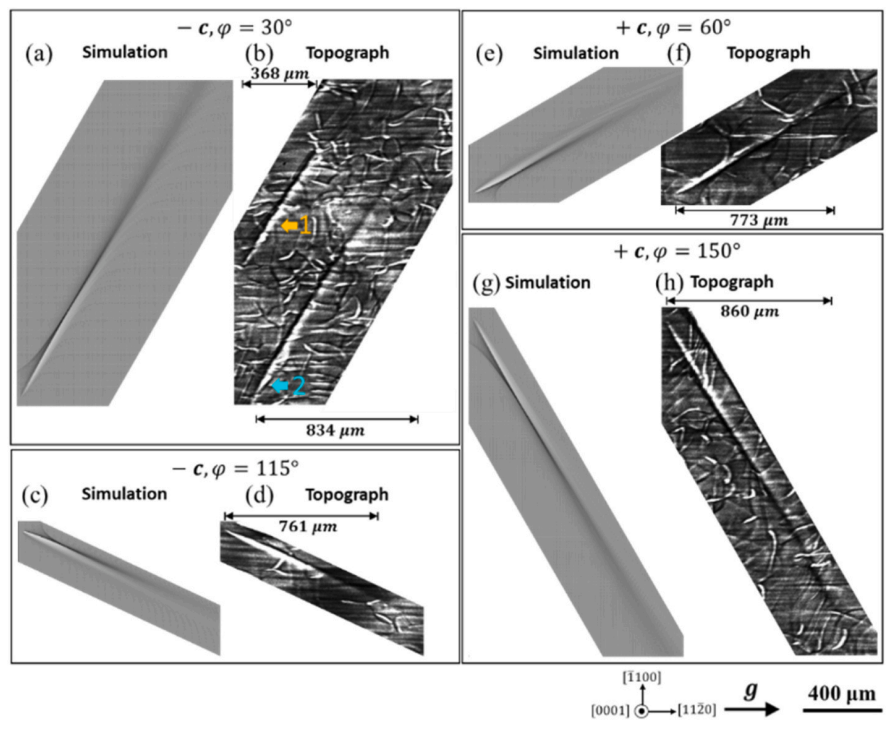
Fig. 19: The ray tracing simulation image of Frank-type dislocations, and the corresponding grazing incidence X-ray topological image are shown.
Fig. 20: The transmitted white beam X-ray topological image of the micropipe on the 6H-SiC wafer, and the ray tracing simulation image are shown.
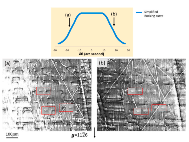
Fig. 21: The grazing incidence monochromatic X-ray topological image of the axially cut sample of 6H-SiC, and the ray tracing simulation image of the BPDs are shown.
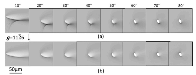
Fig. 22: shows the ray tracing simulation images of BPDs in 6H-SiC axially cut samples at different incident angles.
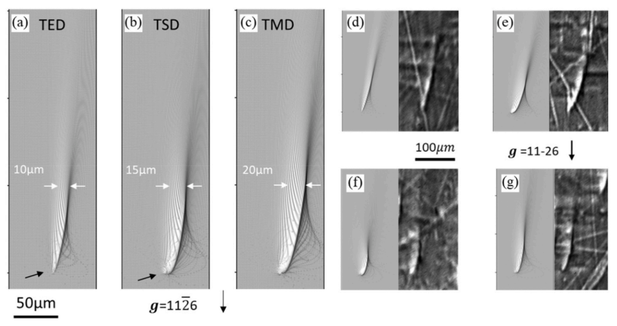
Fig. 23: shows the ray tracing simulation images of TED, TSD and TMDs in 6H-SiC axially cut samples under grazing incidence geometry.
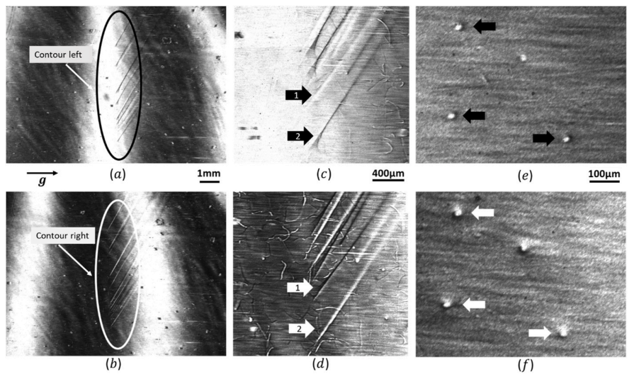
Fig. 24: shows the X-ray topological images of deflected TSDs on different sides of the isoclinic line on the 4H-SiC wafer, and the corresponding ray tracing simulation images.
This article is only for academic sharing. If there is any infringement, please contact us to delete it.
Media Contact
Company Name: Semicera
Email: Send Email
Country: China
Website: https://www.semi-cera.com/

